The entire ESD protection ‘defense system’ of a Smart Band, from sensors to circuits, is a continuous battle against static electricity, the ‘invisible killer.’ Among these protective layers, the Radio Frequency Connector stands as the ‘data throat’ of a Smart Band—it must stably transmit Bluetooth signals and synchronize motion data, while simultaneously confronting the weakest point most susceptible to electrostatic intrusion.
Today, we focus on this critical Connector to dissect the electrostatic protection scheme for the RF Connector, revealing how this ‘throat defense line’ is forged.
Electrostatic Protection for RF Connectors
RF stands for Radio Frequency, a term used for high-frequency electromagnetic waves. In Smart Bands and watches, the RF Connector primarily refers to the wireless Bluetooth or WiFi Connector, which transmits wireless signals or establishes signal connections.
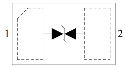
The schematic diagram below typically illustrates the coupling of RF wireless signals and the protection circuit for the RF Connector:
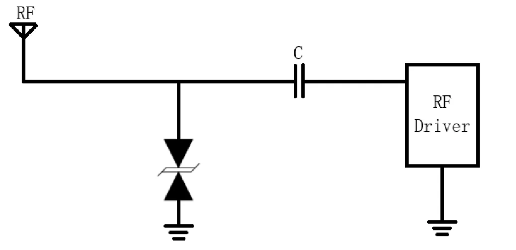
[Diagram of RF Connector Protection Circuit]
Selection of Protection Devices for RF Connectors
The TT0501SB from JY Electronics is an ultra-low capacitance Transient Voltage Suppressor (TVS) designed to provide electrostatic discharge (ESD) protection for high-speed data Connectors. The TT0501SB has a typical capacitance of only 0.35pF, designed to protect parasitic-sensitive systems against over-voltage and over-current transient events. It complies with IEC 61000-4-2 (ESD), Level 4 (±25kV air, ±20kV contact discharge), ultra-fast Charged Device Model (CDM) ESD, and Cable Discharge Event (CDE), among others.
The TT0501SB comes in an ultra-small DFN1006-2L package. Each TT0501SB device can protect a single high-speed data line. It offers system designers flexibility to protect individual lines in applications where arrays are impractical. The combination of small size, ultra-low capacitance, and high ESD robustness makes the TT0501SB an ideal choice for high-speed data ports and high-frequency lines such as USB 2.0 and antenna lines, commonly found in mobile phones and high-definition visual equipment.
The VRWM (Working Reverse Voltage) for the TT0501SB is 5V, meaning when 5V reverse voltage is applied, the diode array remains in reverse blocking state. The VBR (Minimum Avalanche Breakdown Voltage) is 6V; at 25°C, if the applied reverse voltage is below 6V, the diode protection array does not conduct, but when the applied reverse voltage exceeds 6V, the diode turns on and begins to protect the circuit. The VC (Clamping Voltage) is 13V, meaning when peak current flows, the voltage across its terminals is clamped at 13V. The Cj (Junction Capacitance) is 0.35pF, which is the parasitic capacitance of the diode array.
Below are the main performance parameters, internal circuit diagram, and pin configuration diagram for the TT0501SB.
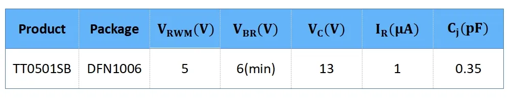
[Main Performance Parameters of TT0501SB]
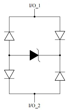
[Internal Circuit Diagram of TT0501SB]
[Pin Configuration Diagram of TT0501SB]
Through today’s content, we have gained a detailed understanding of the electrostatic protection scheme for the RF Connector of Smart Bands, where the ingenious design builds a solid barrier for stable data transmission.”