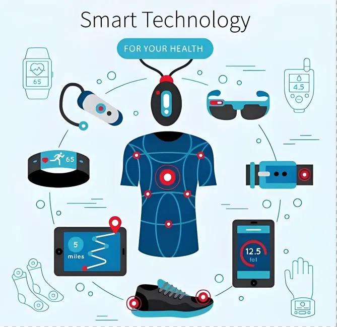
With the explosive proliferation of global AI data centers, large language models, and their downstream applications—particularly since 2025—AI-enabled mobile terminals are penetrating consumer markets at an unprecedented velocity and scale. Driven by highly innovative design paradigms and deep vertical market exploration, a diverse ecosystem of novel intelligent terminals and wearable devices is expanding from China to global markets. AI bedside clocks, AI smart speakers, AI ambient lighting, AI learning cameras, AI smart locks, AI-enabled dolls, AI companion robots, AI learning devices, AI real-time translation earbuds, AI smartwatches, AI audio-visual glasses, AI-AR glasses, AI video intercoms, and embodied AI robots of various form factors are emerging in rapid succession. The common technical characteristics of these products and their constituent modules include high-reliability transmission of standardized RF signals (Wi-Fi, Bluetooth), high-speed signal integrity for USB 3.0 and above interfaces, and dependable operation of ultra-large-scale integrated circuit micro-assemblies—collectively placing increasingly stringent demands on high-speed ESD and surge protection solutions at both the chip and board levels.
As AI bedside clocks, AI learning cameras, AI companion robots, and similar devices enter ordinary households, and as real-time AI translation in TWS earbuds, sub-second heart rate analytics in smartwatches, and AR navigation in AI glasses become part of daily routines, a broad spectrum of “skin-close intelligent terminals” are leveraging motherboard footprints as compact as a fingernail to host multiple chips and complex algorithms. Yet what often goes unnoticed is that static electricity generated by human contact or transient voltage surges during charging can compromise sensitive semiconductor devices within 10 milliseconds, causing abrupt interruption of AI-driven interactions.
Critically, smart wearable devices are evolving toward thinner, lighter, and more highly integrated form factors: the single-side cavity volume of TWS earbuds is now below 1.5 cm³, while smartwatch motherboard areas typically measure under 5 cm². Conventional protection devices present a fundamental trade-off—either excessive physical dimensions that consume scarce PCB real estate, or elevated junction capacitance that degrades high-speed signal integrity—creating an “invisible bottleneck” for the full realization of AI functionality.
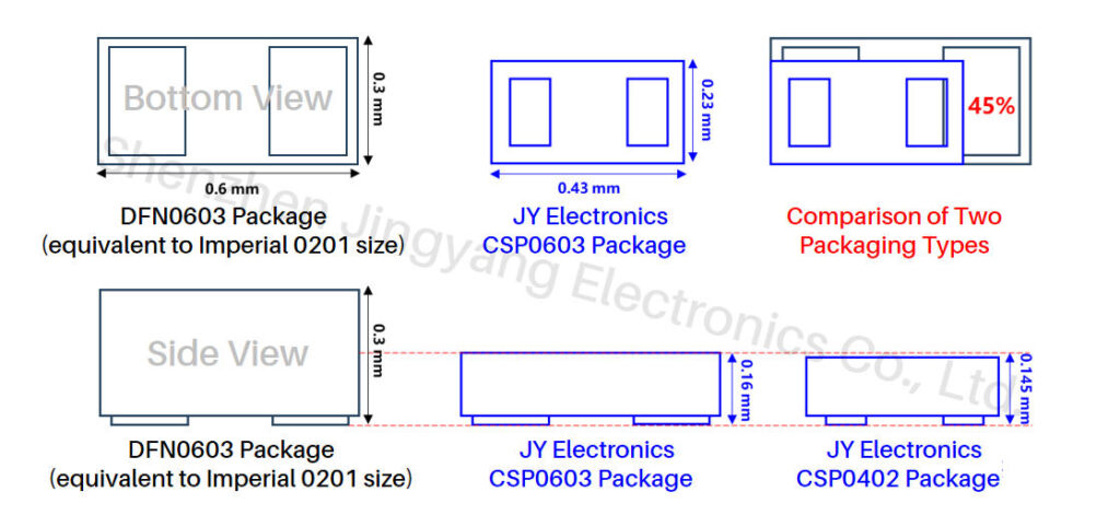
JY Electronics’s high-performance ESD protection series (CSP0402 ultra-compact package, CSP0603 ultra-thin package) establishes a robust protection architecture for micro-scale AI devices, achieving an optimal balance between maximum space efficiency and uncompromised signal integrity. Relative to conventional DFN0603 packaging, JY Electronics’s CSP0402 package reduces footprint by approximately 45%, while the CSP0603 package achieves a 50% reduction in z-axis height.
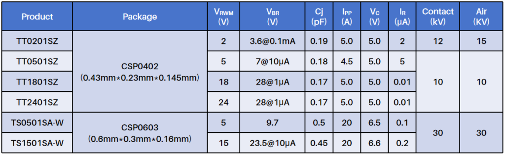
Product Parameters: TT0201SZ, TT0501SZ, TT1801SZ, TT2401SZ, TS0501SA-W, TS1501SA-W
TWS Earbuds: Enabling Zero-Interruption AI Audio Interaction
The Bluetooth 5.3 modules and AI noise-canceling microphones in TWS earbuds exhibit extreme sensitivity to signal interference. JY Electronics’s CSP0402 ESD series, featuring ultra-low junction capacitance, is optimally matched to high-speed RF signal transmission requirements:
- Deployed at charging contacts and capacitive touch interfaces, providing robust immunity to 5A surge currents (8/20μs waveform) during insertion and extraction cycles;
- Capable of withstanding minimum 10kV contact/air electrostatic discharge per IEC 61000-4-2, effectively mitigating static discharge generated by ear canal friction;
- An ultra-compact footprint of approximately 0.1 mm² liberates critical design space for higher-capacity batteries or multi-microphone array configurations.
Smartwatches: Dual-Layer Protection for AI Health Monitoring
The photoplethysmography (PPG) heart rate sensors and SpO₂ modules in smartwatches rely on microcurrent signal acquisition, with AI algorithms requiring continuous, high-fidelity data streams. Any voltage transient can induce signal artifacts and data corruption:
- 2–24V wide operating voltage range precisely aligns with diverse VBUS power architectures, providing active protection at signal interfaces against short-circuit voltage transients;
- Minimum 10kV contact/air ESD protection combined with ultra-low leakage current design not only withstands static discharge from wrist friction and strap contact, but also eliminates parasitic power consumption, extending battery endurance for continuous AI health monitoring;
- Ultra-thin package height below 0.15 mm enables edge-mounting on the motherboard or placement beneath sensor modules without compromising device slimness or haptic response characteristics.
The Micro-Protection Infrastructure of the AI Era: Beyond Wearables
As AI technology continues its penetration into micro-scale terminals—from AI hearing aids to smart rings—every 10% increase in component density correlates with a 30% increase in protection design complexity. This pinhead-scale ESD device constitutes the foundational safety infrastructure for high-density AI hardware:
- Leveraging JY Electronics’s proprietary vertical discharge path architecture, with response time below 1 ns, completing energy dissipation instantaneously upon surge/ESD event detection;
- Compatible with high-speed interfaces including MIPI, USB4, USB Type-C, and antenna feeds, enabling direct integration into AI module signal chains without signal degradation, supporting high-frequency interaction scenarios such as real-time translation and visual search in AR glasses;
- Extended temperature operating range (-55°C to +125°C), ensuring stable AI functionality across environmental extremes from direct solar exposure to severe cold, enabling reliable all-scenario deployment.
In the revolution of AI wearables where smaller form factors enable greater intelligence, protection has never been more mission-critical. JY Electronics’s high-performance ESD series leverages the core advantage of “maximum capability in minimum footprint,” ensuring that intelligence and safety are no longer mutually exclusive design constraints—after all, only by establishing a robust underlying protection architecture can AI truly integrate into every dimension of daily life.
……………………………………………………………………Company Profile……………………………………………………………………
JY Electronics serves a global customer base across the automotive, industrial & power, computing, consumer, and mobile & wearables industries. Our extensive product portfolio includes Schottky diodes, TVS and ESD protection devices, MOSFETs, LDOs, power ICs, battery protection & segment driver ICs, industrial & automotive-grade sensors, high-side switches (HSD), current sensors, and automotive switch input chips. We are committed to continuous innovation, delivering high-quality products that empower our customers to develop energy-efficient and sustainable solutions.
For samples or a quotation, please contact us at market@jy-electronics.com.cn.