
As fast-charging power levels continue to escalate, smartphone and consumer electronics power subsystems face increasingly stringent design constraints: higher power density must be achieved simultaneously with bidirectional current capability, all within the severely limited PCB real estate of modern mainboards. Conventional silicon MOSFETs are approaching fundamental limits in conduction loss, reverse blocking voltage, and package miniaturization. Gallium nitride (GaN) devices, with their inherent advantages in miniaturization and efficiency, are opening new design paradigms.
JY Electronics has introduced the TGE005040B2W22, a bidirectional enhancement-mode GaN power transistor based on silicon-based GaN E-mode HEMT technology. Featuring 40V bidirectional blocking capability, milliohm-level on-resistance, and an ultra-compact wafer-level chip-scale package (WLCSP), the device is optimized for high-side load switching, USB overvoltage protection (OVP) in smartphones, and switched-mode power supply applications.

Four Core Technical Advantages
Addressing Critical Port Design Constraints
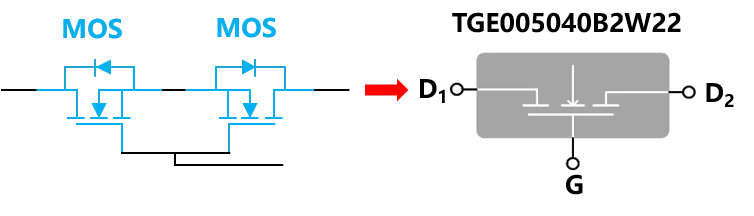
01. Bidirectional Blocking: Simplified Peripheral Circuitry
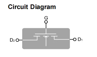
A single TGE005040B2W22 replaces the traditional back-to-back series configuration of two discrete unidirectional MOSFETs required for bidirectional blocking and switching. With 40V bidirectional withstand capability, the device substantially reduces component count and PCB area occupation in applications such as USB OVP and multi-source power switching, while eliminating the additional conduction loss associated with parasitic body diodes.
02. Enhancement-Mode HEMT Architecture: Simplified Gate Drive Design
The TGE005040B2W22 employs enhancement-mode (E-mode) HEMT technology—a normally-off device. This eliminates the requirement for negative gate bias turn-off circuitry, ensuring compatibility with conventional silicon MOSFET gate drive schemes. The result is reduced development complexity and lower system BOM cost, with seamless integration into established power management IC (PMIC) drive architectures.
03. Milliohm On-Resistance + Low Gate Charge: Comprehensive Loss Optimization
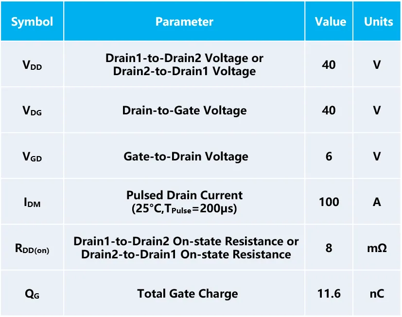
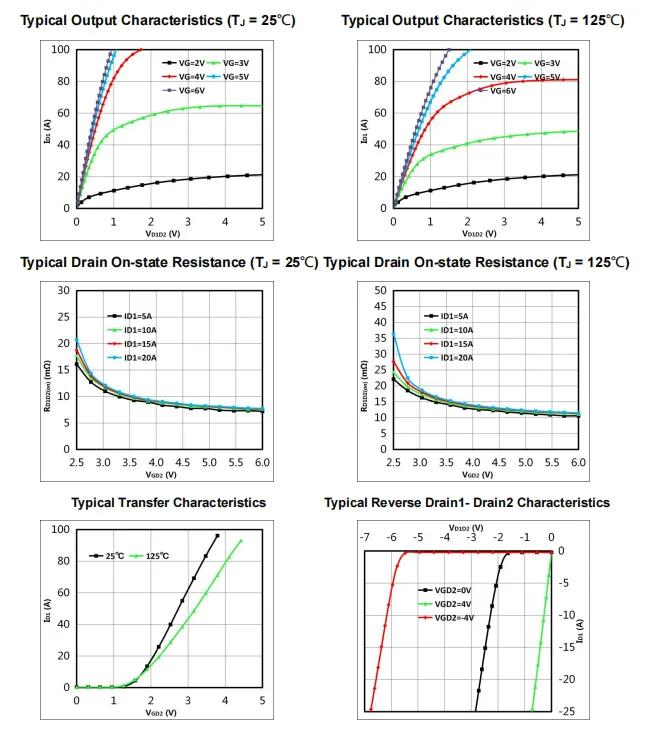
The TGE005040B2W22 achieves a typical on-resistance of 8 mΩ (V_GD = 6V, I_D = 10A), minimizing conduction loss and self-heating under heavy-load conditions for improved overall power conversion efficiency.
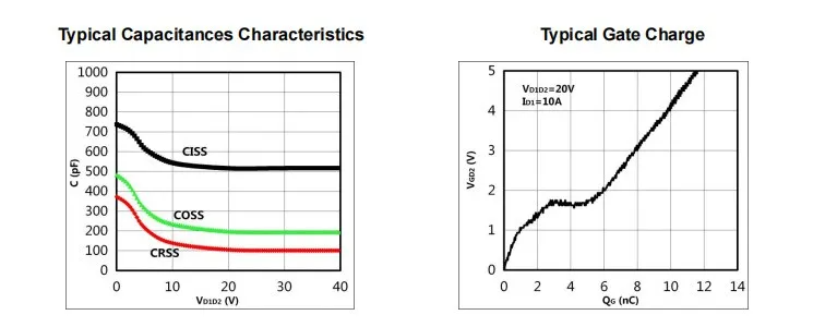
Total gate charge is typically 11.6 nC, with a gate resistance of 0.32 Ω. This combination of low Q_G and R_G enables fast switching transitions with minimal drive loss, supporting high-frequency operation and further optimizing system-level energy efficiency.
04. Ultra-Compact WLCSP Package: Enabling Maximum Density
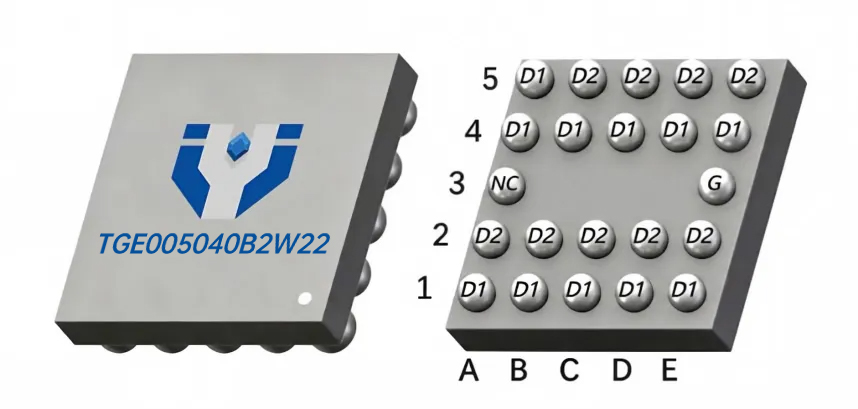
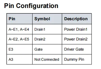
Packaged in a 2.1 mm × 2.1 mm WLCSP outline, the device occupies significantly less volume than conventional DFN alternatives. This form factor is optimized for high-density PCB layouts in smartphones and portable electronics, aligning with industry trends toward miniaturization and reduced z-height.
Key Electrical Parameters
Device Characterization Curves
……………………………………………………………………Company Profile……………………………………………………………………
JY Electronics serves a global customer base across the automotive, industrial & power, computing, consumer, and mobile & wearables industries. Our extensive product portfolio includes Schottky diodes, TVS and ESD protection devices, MOSFETs, LDOs, power ICs, battery protection & segment driver ICs, industrial & automotive-grade sensors, high-side switches (HSD), current sensors, and automotive switch input chips. We are committed to continuous innovation, delivering high-quality products that empower our customers to develop energy-efficient and sustainable solutions.
For samples or a quotation, please contact us at market@jy-electronics.com.cn.