Video connectors are often susceptible to interference from ESD/EOS static electricity. For example, electrostatic surges caused by thunderstorms or electrostatic events during hot-plugging can lead to abnormal video output. This can manifest as an inability to display images, color abnormalities, or flickering screens. In severe cases, the video output chip may need to be replaced by a professional, and the television connected to the connector may even be burned out. Such situations should be avoided whenever possible.
Different display connectors have varying signal paths and control paths. Moreover, the rate at which they transmit signals also differs. As a result, the control chips of each connector require different process technologies and have varying ESD tolerances. Therefore, selecting appropriate ESD protection chip sets for each connector is crucial for effective ESD protection.
DVI Connector
For the DVI connector, the integrated ESD chip TT0514TL can be used for protection. The following figure shows a schematic diagram of the DVI connector connected with an ESD protection chip. The left part is the DVI video decoding and transmission circuit, and the right part is the circuit for displaying DVI video signals on an LCD.
JY Electronics recommends using four TT0514TL integrated ESD diode array protection chips for electrostatic surge protection of the DVI connector.
The specific connection method is shown in the following figure:
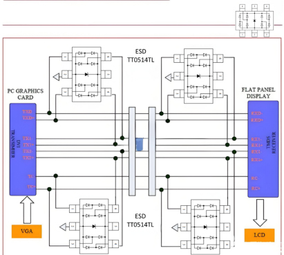
Protection Circuit of TT0514TL Applied to DVI Connector
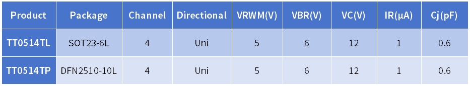
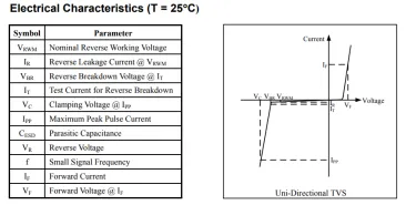
Main Parameter Performance Table of TT0514TL&TT0514TP
The following figure shows the internal circuit diagram of the TT0514TL protection chip. It can be seen that the TT0514TL is mainly composed of a diode array with a certain ESD protection voltage rating. They all have four channels, with a VRWM (maximum continuous working pulse voltage) of 5V, meaning that when a reverse voltage of 5V is applied to the TT0514TL, the diode array is in a reverse-off state; the VBR (minimum avalanche voltage) is 6V, meaning that at 25°C, the reverse voltage applied is less than 6V, and the protected diode array does not conduct; the VC@Ipp of the TT0514TL is 12V@1A, and the Cj is 0.5pF.
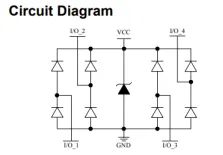
Circuit Diagram of TT0514TL
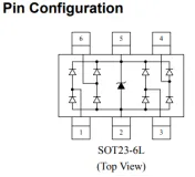
Pin Cross-Section Diagram of TT0514TL
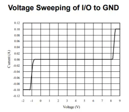
Breakdown Voltage Curve of TT0514TL
TLP Measured Curve of TT0514TL
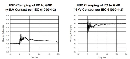
Surge Test Diagram of TT0514TL