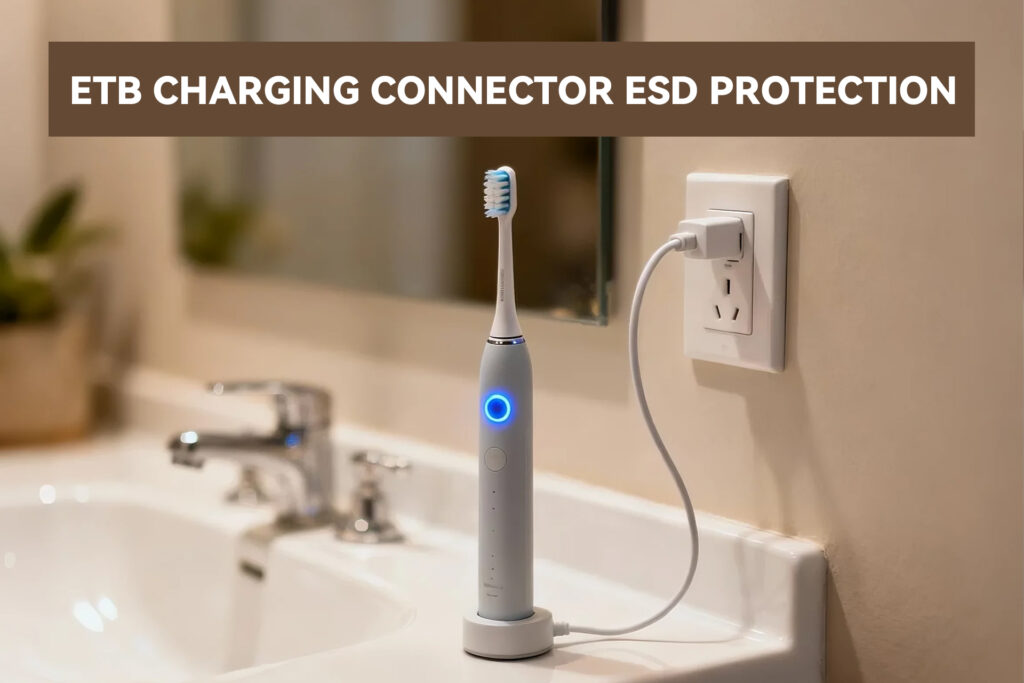
The charging connector of an electric toothbrush is a critical interface, frequently handled by users and exposed to the environment. This makes it highly susceptible to Electrostatic Discharge (ESD) from the human body. An ESD event can damage the sensitive internal charging circuitry, leading to product failure or reduced battery life. Therefore, robust ESD protection is essential for ensuring product reliability and user safety.
1. Selection of ESD Protection Chips for Type-C Connector
Type-C Connector are frequently plugged and unplugged during normal use, making them more susceptible to damage from Electrostatic Discharge (ESD) from the human body. Given the highly integrated chips inside, ESD events can cause component performance degradation or even damage. Furthermore, the advantages of Type-C Connector, such as higher data transmission rates and fast charging capabilities, impose stricter requirements on electrostatic protection.
ESD protection components for Type-C Connector must meet the following three requirements:
- Higher Ipp (Peak Pulse Current)
- Withstand capability of at least IEC 61000-4-2 Contact Discharge 8kV ESD shocks.
- Package size should not be excessively large.
- Lower Vc (Clamping Voltage).
Therefore, JY Electronics recommends the selection of three chips: TT0516ST, TT0374SP-HFx, and TS2451LJ-P.
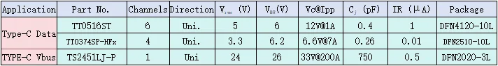
Table 1: Main Performance Parameters of the Three Chips
TT0516ST
As shown in the figure below, the TT0516ST primarily consists of an array of diodes with a certain ESD protection voltage rating. It has 6 channels. The VRWM (Maximum Repetitive Working Voltage) is 5V, meaning that when a reverse voltage of 5V is applied to the TT0516ST, the diode array is in a reverse blocking state. VBR (Minimum Avalanche Breakdown Voltage) is 6V, meaning that at 25°C, the protective diode array does not conduct for reverse voltages below 6V. The VC@Ipp for TT0516ST is 12V@1A, indicating that when a peak current of 1A flows through it, the voltage across it is clamped at 12V. The parasitic capacitance Cj is only 0.4pF, which ensures stable and undistorted high-frequency signal transmission.
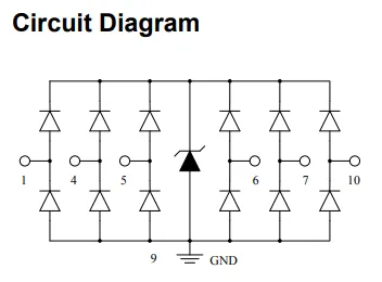
Figure 1: TT0516ST Internal Circuit Diagram
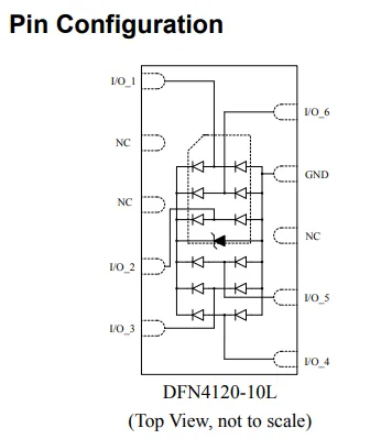
Figure 2: TT0516ST Pin Diagram
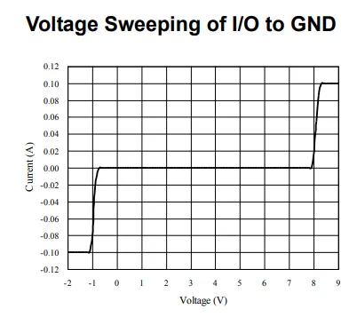
Figure 3: TT0516ST Clamping Voltage Diagram
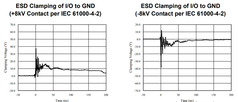
Figure 4: TLP Test Curve for TT0516ST Chip
TT0374SP-HFx
This chip is the latest new product launched by JY Electronics. As shown in the figure below, the TT0374SP-HFx is mainly composed of an array of diodes with a certain ESD protection voltage rating. It has 4 channels. The VRWM (Maximum Repetitive Working Voltage) is 3.3V, meaning that when a reverse voltage of 3.3V is applied to the TT0374SP-HFx, the diode array is in a reverse blocking state. VBR (Minimum Avalanche Breakdown Voltage) is 6.2V, meaning that at 25°C, the protective diode array does not conduct for reverse voltages below 6.2V. The VC@Ipp for TT0374SP-HFx is 6.6V@7A, indicating that when a peak current of 7A flows through it, the voltage across it is clamped at 6.6V. Notably, the operating leakage current IR of the TT0374SP-HFx is only 0.01μA, thus minimizing circuit power consumption.
Performance Highlights:
- To ensure the integrity of high-speed signal data transmission, this new product features ultra-low capacitance (Capacitance between I/O and GND as low as 0.26 pF at VR=0V, f=1MHz).
- Utilizing JY Electronics’s proprietary Deep Hysteresis Leading Edge patent technology, the new product exhibits a low clamping voltage (8/20μs test waveform: IPP=7A, Vc=6.6V). Compared to conventional zero-hysteresis or shallow-hysteresis devices, deep-hysteresis devices offer superior circuit protection.
- It has high ESD withstand capability, able to endure 14kV contact discharge and 15kV air discharge shocks per IEC 61000-4-2 testing.
- It features a compact, four-channel integrated array DFN2510 package, which minimizes the space occupied on the PCB and offers lower cost.

Figure 5: TT0374SP-HFx Pin Configuration Diagram
TS2451LJ-P
As shown in the figure below, the TS2451LJ-P is composed of a single diode, thus it has only 1 channel and is a unidirectional device. As shown in Table 1, the TS2451LJ-P is a unidirectional 24V protection device in a DFN2020-3L package, boasting strong surge circuit tolerance. Its IPP (Peak Pulse Current) reaches 200A, allowing it to maintain normal operation under instantaneous large current surges.
The VRWM (Maximum Repetitive Working Voltage) is 24V, meaning that when a reverse voltage of 24V is applied to the TS2451LJ-P, the diode array is in a reverse blocking state. VBR (Minimum Avalanche Breakdown Voltage) is 26V, meaning that at 25°C, the protective diode array does not conduct for reverse voltages below 26V. The VC@Ipp for TS2451LJ-P is 33V@200A, indicating that when a peak current of 200A flows through it, the voltage across it is clamped at 33V. The leakage current IR is only 0.5μA, enabling low-power operation.
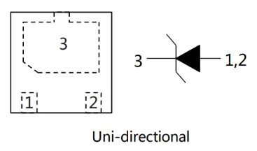
Figure 6: TT2451LJ-P Circuit Schematic Diagram
2. Selection of ESD Protection Chips for USB Connector
USB 2.0 High-Speed Connector
- To ensure high-speed signal integrity during USB 2.0 data transmission, ESD protection components with low capacitance must be selected.
- They must have high ESD withstand capability, capable of enduring at least 8kV contact discharge shocks as specified by IEC 61000-4-2.
- ESD clamping voltage is a critical parameter; a lower clamping voltage indicates better protection performance.
ESD Protection Device placed at the VBUS line (generally unidirectional):
Junction capacitance size is not a major concern.
Maximum reverse working voltage: 5V
Breakdown voltage: around 6V
Clamping voltage: around ten volts.
ESD Protection Device placed on the differential signal lines (generally bidirectional), to prevent static electricity from damaging the chip via the signal lines:
Junction capacitance should be as small as possible to avoid affecting the transmission rate, ideally below 1pF.
Maximum reverse working voltage: 5V
Breakdown voltage: around 6V
Clamping voltage: around ten volts.
To meet these requirements, JY Electronics offers the following products for USB 2.0 ESD/EOS protection: TT0514TL, TT0521SB, and TS0511LE.
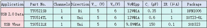
Table 2: Main Performance Parameters of TT0514TL, TT0521SB, and TS0511LE
TT0521SB
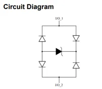
Figure 7: TT0521SB Circuit Schematic Diagram
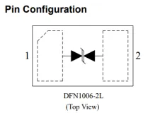
Figure 8: TT0521SB Pin Configuration Diagram
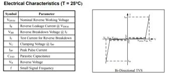
Figure 9: TLP Curve for TT0521SB Chip
TT0514TL

Figure 10: TT0514TL Circuit Schematic Diagram

Figure 11: TT0514TL Pin Configuration Diagram
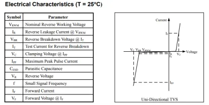
Figure 12: TLP Curve for TT0514TL Chip
TS0511LE
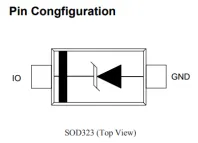
Figure 13: TS0511LE Pin Configuration Diagram
Figure 14: TS0511LE Packaged Chip Schematic Diagram
USB 3.0 High-Speed Connector
For the higher speed and stability of USB 3.0, JY Electronics recommends its latest new ESD product, the TT0374SP-HFx, which offers the following advantages:
To ensure the integrity of high-speed signal data transmission, this new product features ultra-low capacitance (Capacitance between I/O and GND as low as 0.26 pF at VR=0V, f=1MHz).
Utilizing our proprietary Deep Hysteresis Leading Edge patent technology, the new product exhibits a low clamping voltage (8/20μs test waveform: IPP=7A, Vc=6.6V). Compared to conventional zero-hysteresis or shallow-hysteresis devices, deep-hysteresis devices offer superior circuit protection.
It has high ESD withstand capability, able to endure 14kV contact discharge and 15kV air discharge shocks per IEC 61000-4-2 testing.
It features a compact, four-channel integrated array DFN2510 package, which minimizes the space occupied on the PCB and offers lower cost.
Notably, the operating leakage current IR of the TT0374SP-HFx is only 0.01μA, thus minimizing circuit power consumption.
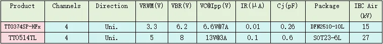
Table 3: Main Performance Parameters of TT0374SP-HFx and TT0514TL Chips
TT0514TL
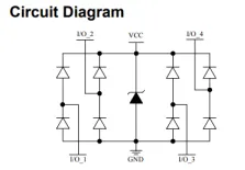
Figure 15: TT0514TL Circuit Schematic Diagram
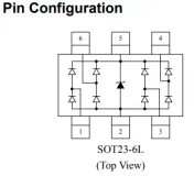
Figure 16: TT0514TL Pin Configuration Diagram
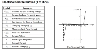
Figure 17: TLP Curve for TT0514TL Chip
TT0374SP-HFx
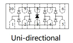
Figure 18: TT0374SP-HFx Pin Configuration Diagram