1.ESD Protection Solution for USB 2.0
 |  |
As illustrated in Figure 1, a schematic of an ESD protection solution for a USB interface, USB Controller/Charger denotes the host-side controller or power delivery IC, while the USB Port represents the downstream connector on a device. The ESD protection device from JY Electronics is strategically placed between the controller and the port to provide robust protection.
For instance, during a hot-plug event, an Electrostatic Discharge (ESD) transient generates a high-voltage, high-current surge on the data and power lines. The ESD protection device from JY Electronics provides a low-impedance path to shunt this transient current to ground, while clamping the voltage to a safe level. This safe level is defined as the Clamping Voltage (Vc), a critical parameter specific to each ESD protection device model.
Figure 1 details two application scenarios for single and dual USB 2.0 port protection using solutions from JY Electronics. The left diagram shows a single-port configuration utilizing two TT0521SB devices and one TS0511LE device. The I/O pins of the two TT0521SB devices are connected to the D+ and D- differential data lines, respectively. The I/O pin of the TS0511LE is connected to the VBUS power line, with all ground pins tied to system ground (GND).
The right diagram presents a dual-port solution, which can be implemented with a single integrated TT0514TL device from JY Electronics. Pins 1, 3, 4, and 6 are connected to their respective data lines, while pins 2 and 5 are connected to VBUS and GND.
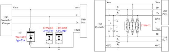
Figure 1: ESD Protection Application Circuit for a USB 2.0 Port
2.ESD Protection Solution for USB 3.0
USB 3.0 architecture expands upon the 2.0 standard by incorporating two additional high-speed differential pairs: TX± for data transmission and RX± for data reception. This significantly increases the data bandwidth, which in turn necessitates ESD protection devices with ultra-low capacitance to maintain signal integrity. The recommended solution from JY Electronics consists of two TT0374SP-HFx devices and one TT0514TL device.
As depicted in Figure 2, the TT0514TL’s role in protecting the VBUS line is consistent with the USB 2.0 application. The two TT0374SP-HFx devices from JY Electronics are dedicated to protecting the SuperSpeed data lines. Pins 1, 2, 4, 5, 6, 7, 9, and 10 are connected to the TX± and RX± differential pairs. The remaining pins, 3 and 8, are tied to ground.
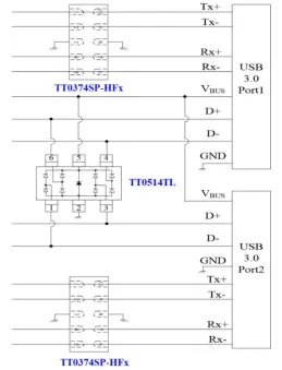
Figure 2: Application Circuit of TT0374SP-HFx and TT0514TL Devices on a USB 3.0 Port
