As consumers demand higher data transfer speeds and stability from electronic products, manufacturers are increasingly seeking advanced electrostatic discharge (ESD) protection for various interfaces. The potential hazards of electrostatic discharge to electronic products/equipment include:

- Electronic device damage: ESD/surge can cause instantaneous high voltage that exceeds the tolerance of control chips or circuits, leading to damage to high-speed interfaces or circuit boards, rendering the device inoperative.
- Data loss or corruption: ESD/surge can interfere with signal transmission, leading to errors or loss of data, affecting the functionality and performance of products/equipment.
TT0361SA-HFx – Designed for High-Speed Signal Lines
Therefore, to protect the functional integrity of electronic products from the destructive effects of surge electrostatic discharge, the use of electrostatic surge suppressors (ESD, Electro-Static discharge) or transient voltage suppressors (TVS) and other protective devices becomes crucial.
Selected Protection Solution TT0361SA-HFx
JY Electronics introduces the new ESD product TT0361SA-HFx to protect high-speed signal transmission interfaces (such as USB3.2, USB4.0, Thunderbolt, HDMI2.0, HDMI2.1, etc.) from ESD/surge damage, with the following advantages:
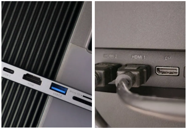
- To ensure the integrity of high-speed signal data transmission, the new product features ultra-low capacitance (at VR=0V, f = 1MHz: IO-GND capacitance as low as 0.18 pF).
- Utilizing our company’s unique deep snapback leading-edge patent technology, the new product has an ultra-low clamping voltage (8/20μs test waveform: IPP=6A, Vc=6 V), providing better protection performance for circuits compared to conventional non-snapback and shallow snapback ESD.
- It has a high ESD tolerance, capable of withstanding 12kV contact discharge and 15kV air discharge ESD shocks as tested by IEC 61000-4-2.
- The compact design features lead-free DFN0603 surface-mount packaging, which minimizes the space occupied on the PCB and reduces costs.


JY Selected Electrostatic Protection Solution
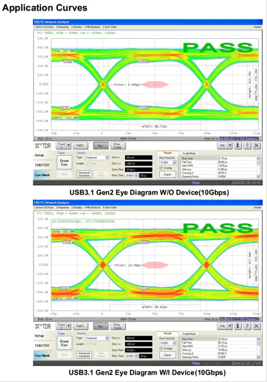
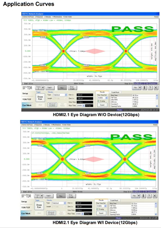
Eye Diagram Test Curves
Layout Design Considerations
1.TVS devices should be laid out as close as possible to the input end of the disturbance source (near the panel).
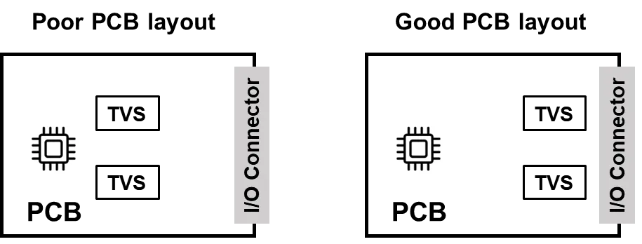
2.The wires connected to the TVS devices should be as short and thick as possible to reduce the parasitic inductance of the wires and maintain a low-impedance loop. Ensure that the TVS device wiring is shorter than the wiring of the protected object to ensure that external pulse interference is released through the TVS device.
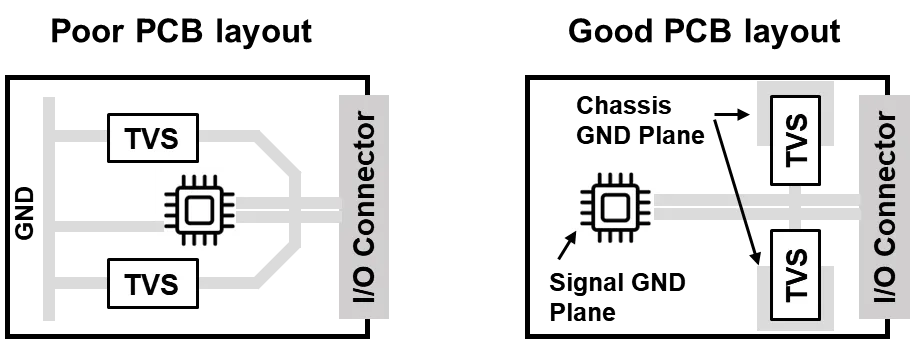
3.The TVS device protection circuit should directly discharge energy to the protection ground. It is not recommended to connect it directly to the working signal ground to avoid causing signal rebound on the working ground plane.
