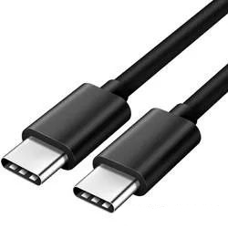
Type-C Interface Introduction
The Type-C interface is a brand-new form of USB interface widely used in USB 3.X and USB 4.0. The Type-C interface has many advantages, such as reversible charging without distinguishing between positive and negative, allowing a larger maximum current during charging, etc. Currently, the Type-C interface on mobile phones, in addition to charging, can also transfer data with computers, act as audio and network input-output interfaces through adapter cables, etc. Type-C has rich interface resources and can meet various application scenario needs.
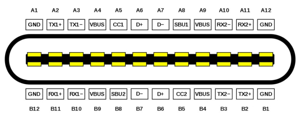
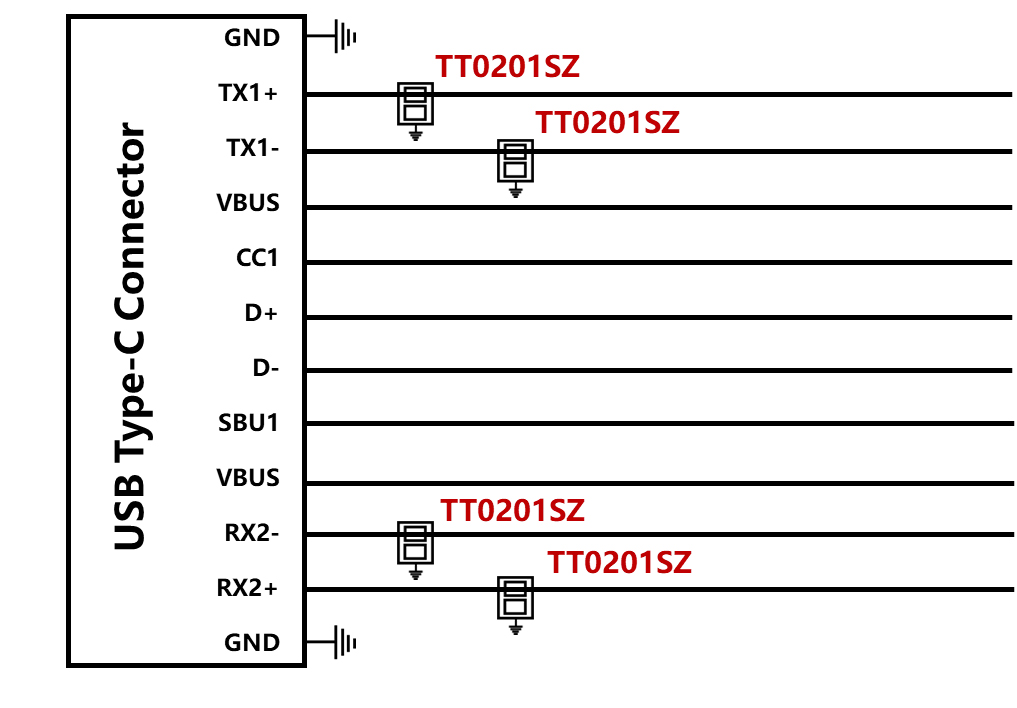
USB Type-C Connector End View
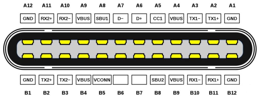
USB Type-C Extraction End View
JY Electronics Selection Recommendation: TT0201SZ
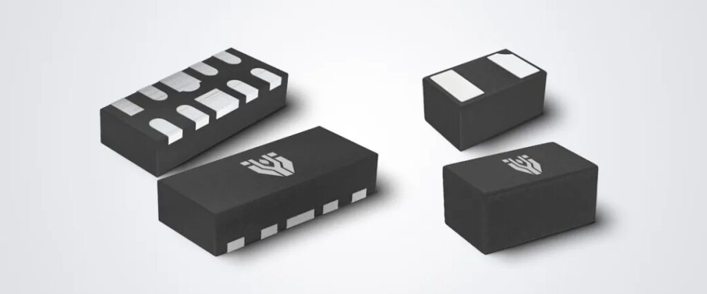
TT0201SZ
With the semiconductor process technology becoming smaller, semiconductor products are becoming more precise, and the main chip’s requirement for electrostatic discharge (ESD) protection capability is getting higher. When selecting ESD/EOS protection components for high-speed interfaces like USB 3.X and USB 4.0, consider the following points:
- To ensure the integrity of high-speed signals transmitted via USB 3.X and USB 4.0, ESD protection components with low capacitance are required.
- High ESD voltage endurance is crucial, with a minimum requirement to withstand the ESD shocks from 8kV contact discharge as specified in IEC 61000-4-2.
- For low-voltage chips under advanced process technology, ESD with lower turn-on voltage is more conducive to chip protection.
- A lower clamping voltage indicates better protective performance.
- Smaller packaging to save PCB space in consumer electronics or wearable devices.
To meet the above requirements, JY Electronics has launched the transient suppression diode product TT0201SZ (mainly for the protection of the TX and RX ends of USB 3.X and USB 4.0) to protect against electrostatic discharge (ESD) damage. It features the industry’s smallest package CSP0402 and ultra-low capacitance (typical value of 0.19 pF at VR=0V, f = 1MHz), low turn-on voltage (VBR=3.6V@0.1mA), and low clamping voltage that allows for rapid response to prevent ESD damage. TT0201SZ also meets the IEC 61000-4-2 standard for 12 KV contact discharge and 15KV air discharge.
The compact design of TT0201SZ allows it to protect high-speed interfaces while minimizing the space occupied on the PCB. Typical applications include providing ESD protection for high-speed interfaces in IoT modules, smartphones, external storage devices, portable wearable devices, TWS earphones, ultrabooks/laptops, tablets/e-readers, and security modules.
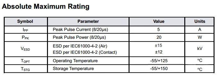
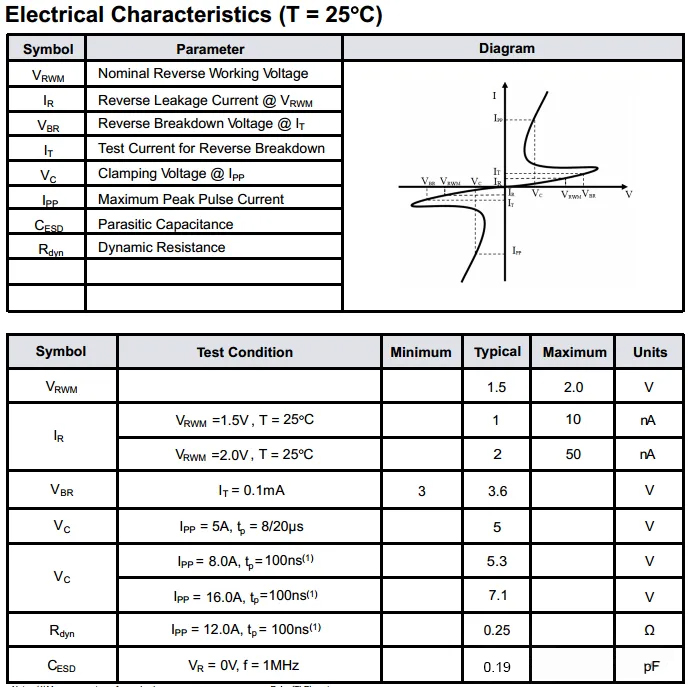

TT0201SZ Datasheet
Layout Design Considerations:
- Place ESD protection components as close as possible to I/O connectors to reduce ESD grounding paths and enhance protection performance.
- In USB 3.X and USB 4.0 applications, ESD protection components should be placed between the AC-coupling capacitors on the TX differential channel and the I/O connectors, preventing any direct current from flowing through the ESD protection components, thus preventing any potential latch-up risks.
- Use bent traces whenever possible to avoid unnecessary reflections.
- Maintain equal trace lengths between the positive and negative lines of differential data channels to prevent the generation of common mode noise and impedance mismatch.