As consumers demand higher data transfer speeds and stability from electronic products, manufacturers are increasingly seeking advanced electrostatic discharge (ESD) protection for various interfaces. The potential hazards of electrostatic discharge to electronic products/equipment include:
- 1、Electronic device damage: ESD/surge can cause instantaneous high voltage that exceeds the tolerance of control chips or circuits, leading to damage to high-speed interfaces or circuit boards, rendering the device inoperative.
- 2、Data loss or corruption: ESD/surge can interfere with signal transmission, leading to errors or loss of data, affecting the functionality and performance of products/equipment.

Therefore, to protect the functional integrity of electronic products from the destructive effects of surge electrostatic discharge, the use of electrostatic surge suppressors (ESD, Electro-Static discharge) or transient voltage suppressors (TVS) and other protective devices becomes crucial.
Selected Protection Solution TT0374SP-HFx
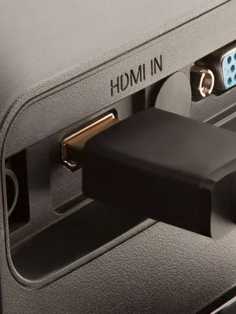
JY Electronics introduces the new ESD product TT0374SP-HFx to protect high-speed signal transmission interfaces (such as USB3.1, USB3.2, Thunderbolt, HDMI2.0, etc.) from ESD/surge damage. The product offers the following advantages:
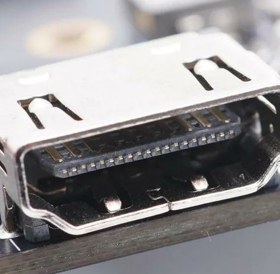
- 1、To ensure the integrity of high-speed signal data transmission, the new product features ultra-low capacitance (at VR=0V, f = 1MHz: IO-GND capacitance as low as 0.26 pF).
- 2、Utilizing our company’s unique deep snapback leading-edge patent technology, the new product has a lower clamping voltage (8/20μs test waveform: IPP=7A, Vc=6.6 V), providing better protection performance for circuits compared to ordinary non-snapback and shallow snapback devices.
- 3、It has a high ESD tolerance, capable of withstanding 14kV contact discharge and 15kV air discharge ESD shocks as tested by IEC 61000-4-2.
- 4、The compact design features a four-channel integrated array DFN2510 package, which minimizes the space occupied on the PCB and reduces costs.
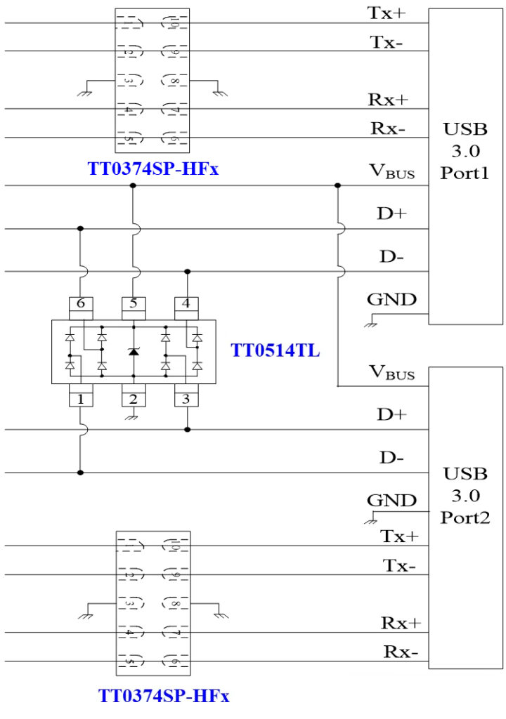
(JY Selected Electrostatic Protection Solution)

ESD Performance Parameter Table for Signal and Power Protection
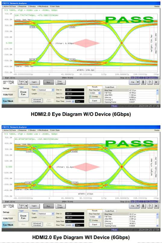
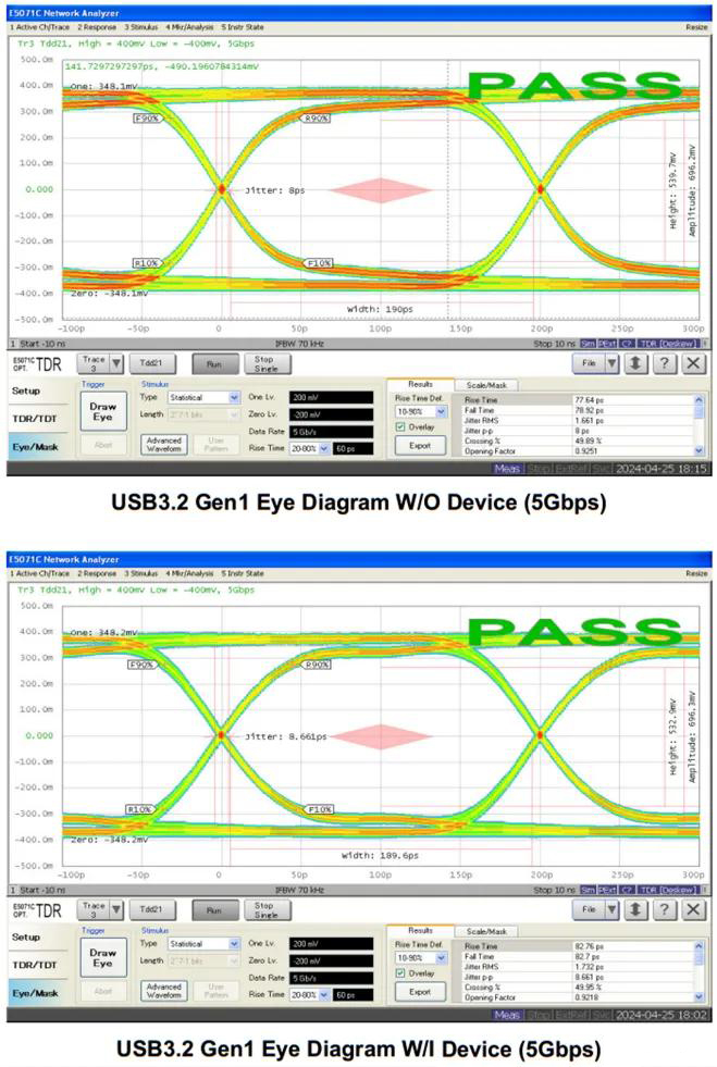
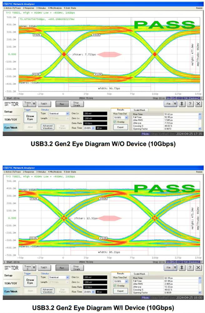
(Eye Diagram Test Curves)
Layout Design Considerations:
- 1、Place ESD protection devices as close as possible to I/O connectors to reduce ESD grounding paths and enhance protection performance.
- 2、PCB routing should preferably have rounded corners or 45-degree angles, avoiding right-angle wiring to prevent unnecessary reflections.
- 3、Maintain equal trace lengths between the positive and negative lines of differential data channels to avoid the generation of common mode noise and impedance mismatch.