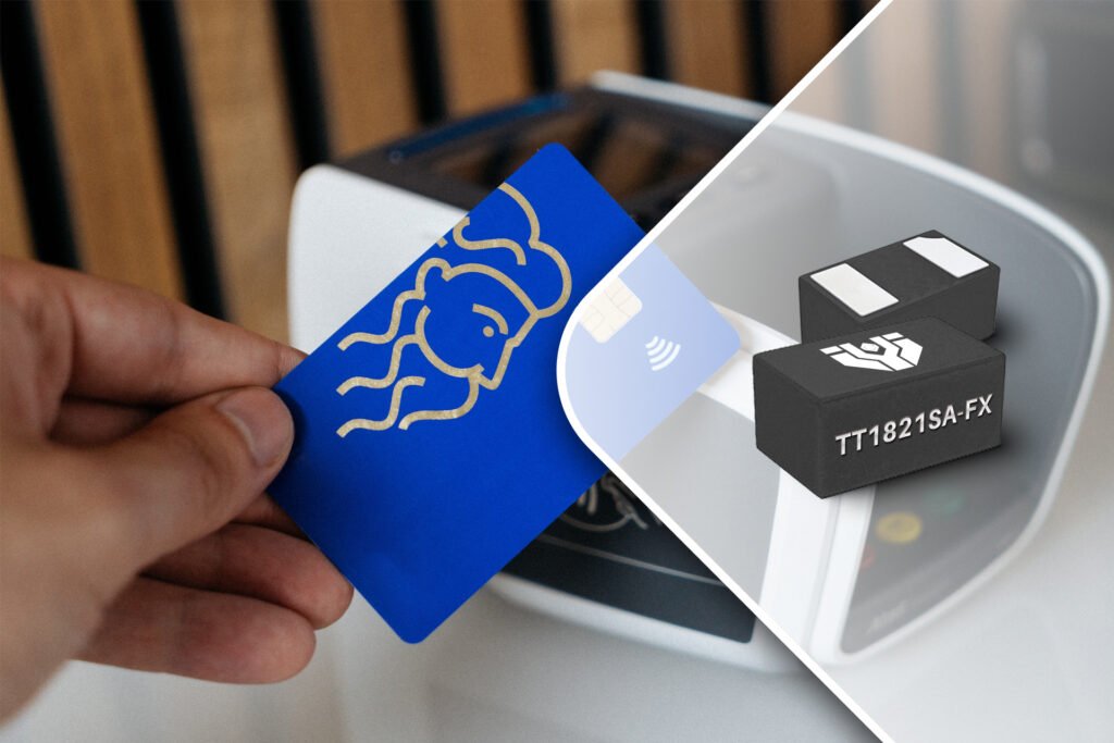
- NFC Introduction
NFC (Near Field Communication), also known as “proximity communication” or “short-range wireless communication,” is a high-frequency wireless communication technology designed for short-distance interactions. It evolved from the integration of contactless Radio Frequency Identification (RFID) and interconnectivity technologies. Devices utilizing NFC technology can exchange data when in close proximity, enabling applications such as mobile payments, electronic ticketing, access control, mobile identity recognition, and anti-counterfeiting, primarily through mobile terminals like smartphones.
NFC devices can engage in active or passive mode data exchange. The initiator of NFC communication is referred to as the initiator, while the receiver is termed the target. Active communication entails both the initiator and target generating their own radio frequency fields during data transmission. The initiator generates its radio frequency field while sending data, while the target, in a listening mode, receives the initiator’s data by deactivating its own radio frequency field. After the initiator completes data transmission, it deactivates its radio frequency field and enters a listening mode, awaiting data from the target. In passive mode, the initiator provides the radio frequency field throughout the communication process. It can choose transmission speeds of 106kbps, 212kbps, or 424kbps to send data to the target. The target doesn’t need to generate a radio frequency field but utilizes load modulation technology to transmit data back to the initiator at the same speed.
- ESD Protection Requirements for NFC Antennas
NFC technology is primarily applied in compact and portable products such as smartphones, tablets, and wristbands. Its antenna is usually situated within the battery, connected to the NFC chip via small contacts. ESD protection is crucial for the NFC device interface, as electrostatic discharge (ESD) can disrupt normal device operation and even lead to device damage. Accumulated charges on the device’s metallic components can create an electric field around the interface, resulting in ESD. TVS/ESD diodes are employed to safeguard the NFC device interface from ESD threats.
Electronic products employing NFC technology are lightweight and portable, necessitating small ESD components. Commonly, DFN0603-2L (imperial 0201) or even CSP0402-2L (imperial 01005) packages are used to reduce PCB space effectively.
Considering signal integrity on high-frequency antennas, parasitic capacitance should be minimized, generally being less than 0.5 pF, with good linearity.
NFC antenna transmission often requires high power. Therefore, ESD protection devices should show a relatively high VRWM value, typically around 18V/24V, and be bidirectional.
ESD components need to withstand 8kV contact tests according to IEC 61000-4-2 for electrostatic resistance.
Protective components should possess sufficiently low clamping voltages to provide effective safeguarding for downstream circuits.
- JY ELECTRONICS’ Recommended Selection: TT1821SA-Fx/TT1821SA-Ft
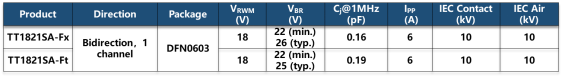
To meet these requirements, JY ELECTRONICS unveils two models, TT1821SA-Fx and TT1821SA-Ft, as ESD protection devices for NFC antennas. These products feature a Snap-back structure, ultra-low capacitance of as low as 0.16 pF (TT1821SA-Fx) and 0.19 pF (TT1821SA-Ft), a clamping voltage of 6V at 6A, and IEC 61000-4-2 compliance at ±10kV (contact) and ±10kV (air).
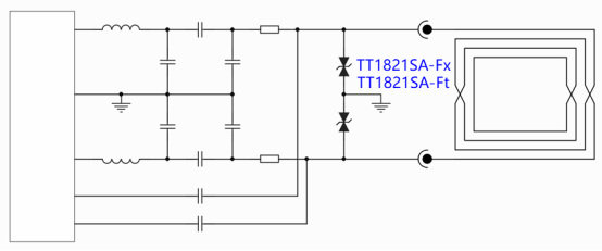
Example Diagram of NFC Interface Application
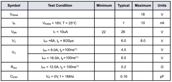
TT1821SA-Fx Specifications
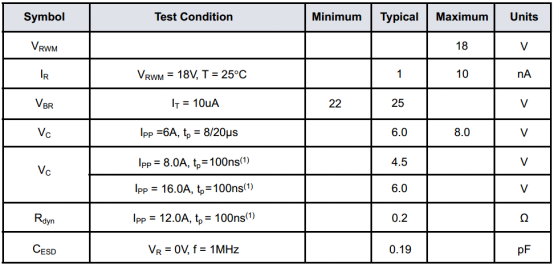
TT1821SA-Fx Specifications
Choose TT1821SA-Fx/TT1821SA-Ft to provide reliable and efficient ESD protection for your NFC antenna.