JY ELECTRONICS, the essential Expert in Circuit and System Protection, today launched the expansion of its ESD protection product portfolio with the introduction of the High-Efficiency Bidirectional Single-Channel ESD Protection Devices for USB 3.X and USB 4.0 (Targeting Type-C Interfaces).
- Type-C Interface Introduction
The Type-C interface represents a novel form of USB interface that finds extensive application in USB 3.X and USB 4.0 technologies. The Type-C interface exhibits numerous advantages, such as reversible charging, allowing insertion without regard to orientation, and support for higher maximum current during charging. Presently, the Type-C interface on mobile devices serves purposes beyond charging, enabling data exchange with computer terminals and serving as an audio input-output interface through adapter cables. With its versatile interface capabilities, Type-C caters to various application.

USB Type-C connector view
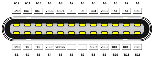
USB Type-C connector view
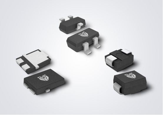
JY ELECTRONICS new product:TT0241SA-Fx
When selecting ESD/EOS protection components for USB 3.X and USB 4.0 high-speed interfaces, several factors should be taken into consideration:
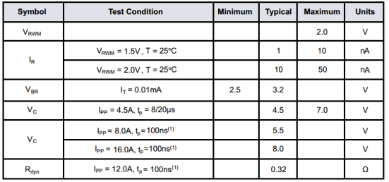
To ensure the integrity of high-speed signals transmitted via USB 3.X and USB 4.0, it’s essential to opt for ESD protection components with low capacitance.
High ESD voltage endurance is crucial, with a minimum requirement to withstand the ESD shocks from 8kV contact discharge as specified in IEC 61000-4-2.
Having a low clamping voltage is advantageous, as it signifies better protective performance.
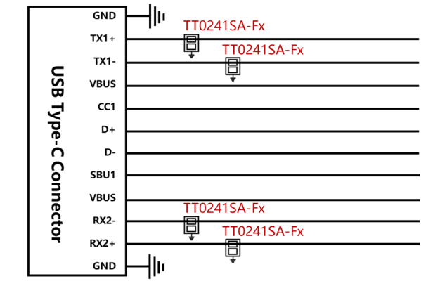
To address these requirements, JY ELECTRONICS has unveiled its TT0241SA-Fx , optimized for TX and RX protection, specifically tailored to USB 3.X and USB 4.0 interfaces. This line incorporates reduced capacitance values and lower clamping voltages for enhanced performance.


- Consideration for Layout design:
Place ESD protection devices in close proximity to I/O connectors whenever possible to minimize ESD grounding path and enhance protection performance.
For USB 3.X and USB 4.0 applications, the position of ESD protection devices between the AC-coupling capacitors in the TX differential channel and the I/O connectors. This configuration prevents any direct current from flowing through the ESD protection devices, mitigating potential latch-up risks.
Employ bent traces whenever feasible to avoid unnecessary reflections.
Maintain equal trace lengths between the positive and negative lines of differential data channels to prevent the generation of common mode noise and impedance mismatch.
