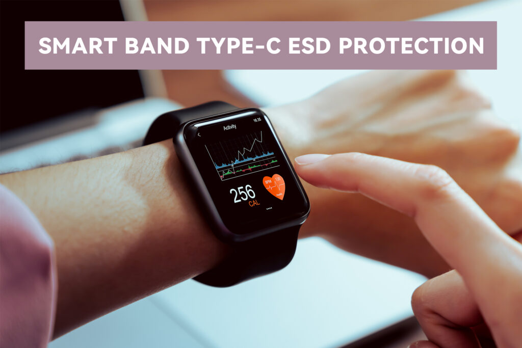
Today, we focus on ESD protection solutions for smart bands and examine how these “invisible armors” safeguard the final line of defense for device stability.
Smart Band ESD Protection Principles
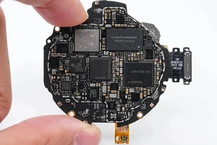
Smart bands, worn directly on the skin, are susceptible to ESD due to the inherent static charge of the human body. Daily contact and charging processes expose them to ESD interference. Internal components such as sensor circuits, batteries, buttons, charging ports, Bluetooth, WiFi, and USB interfaces are all vulnerable to varying degrees of ESD, potentially causing:
Unreliable Bluetooth connections with communication devices like smartphones, leading to data transfer issues.
Inaccurate step counting due to high-frequency electromagnetic interference affecting internal accelerometers in high-frequency electromagnetic environments.
Damage to sensitive circuits, including Bluetooth and USB interfaces, caused by ESD interference.
Therefore, ESD circuit protection is crucial for miniature devices like smart bands and watches. Furthermore, the selection of ESD protection components has additional requirements:
1、Low Capacitance: To avoid interfering with high-speed data transmission and ensure the ESD protection doesn’t disrupt normal circuit function.
2、Low Clamping Voltage: To effectively protect the most sensitive circuits. During an ESD event, the protection device must promptly divert and dissipate the transient voltage, protecting sensitive circuits like USB interfaces from damage.
- Compact Size: To accommodate the limited available space in wearable devices.
USB Interface ESD Protection
ESD protection of the USB interface is of paramount importance in smart bands and watches. Currently, most use Type-C interfaces.
Type-C Interface
Also known as the USB Type-C connector, this is the latest USB form factor standard. The Type series includes Type-C, Type-A, and Type-B interfaces. Compared to Type-A and Type-B, Type-C is significantly smaller, approximately one-third the size. The Type-C interface supports reversible plug orientation, eliminating the frustration of incorrect insertion. It can withstand 10,000 repeated insertions and removals. The maximum data transfer rate reaches 10 Gbit/s, aligned with the USB 3.1 standard. Type-C also offers excellent expandability, supporting alternate modes. A single Type-C port can handle power, USB, signals, and various other interfaces, simplifying connectivity with a single cable.
Type-C interfaces are frequently plugged and unplugged during normal use, increasing their susceptibility to damage from human body ESD. The highly integrated chips inside are vulnerable to performance degradation or even complete failure due to ESD. The higher data transfer rates and fast charging capabilities of Type-C also increase the demands on ESD protection.
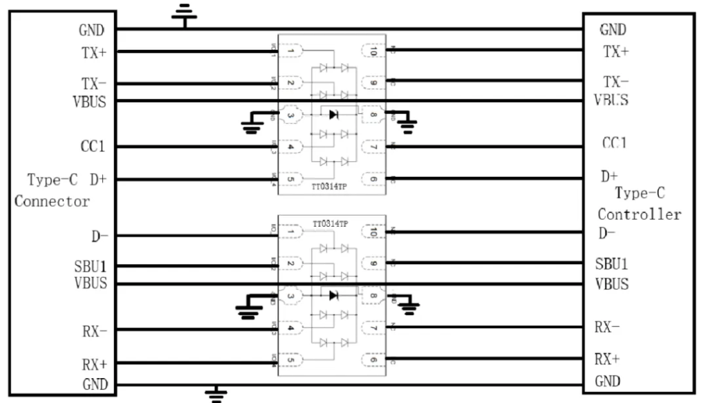
Type-C Interface Protection Circuit Diagram
Recommended Type-C Protection Device
JY Electronics TT0314TP is a low-capacitance ESD protection device designed for high-speed data interfaces. The TT0314TP is packaged in a RoHS-compliant and halogen-free 2.5mm x 1.0mm x 0.55mm DFN2510-10L package. This device integrates eight surge-rated, ultra-low capacitance steering diodes and a TVS in a single package. Under transient conditions, the steering diodes direct the transient signal to the positive power line or ground. TT0314TP complies with IEC61000-4-2 (ESD), Level 4 (±15kV air, ±8kV contact discharge), IEC61000-4-5 (Lightning) (5A, 8/20μs), and more.
The TT0314TP has a VRWM of 3.3V. With a reverse voltage of 3.3V applied to the TT0314TP, the diode array remains in a reverse blocking state. The avalanche voltage is 7V, meaning that when the applied reverse voltage is below 7V, the protection diode array does not conduct. When the applied reverse voltage exceeds 7V, the diodes conduct and begin protecting the circuit. Vc@Ipp (clamping voltage @ impulse current) is 3.5V @ 5A, meaning that a peak current of 5A is permissible, clamping the voltage across the protected circuit to 3.5V. Cj is 0.7pF, representing the parasitic capacitance of the diode array, ideally suited for the high-speed data transfer characteristics of USB 3.0, ensuring data integrity.
Below are the main performance parameters, internal circuit diagram, and pin configuration diagram of the TT0314TP.
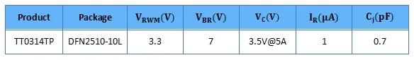
TT0314TP Main Performance Parameters
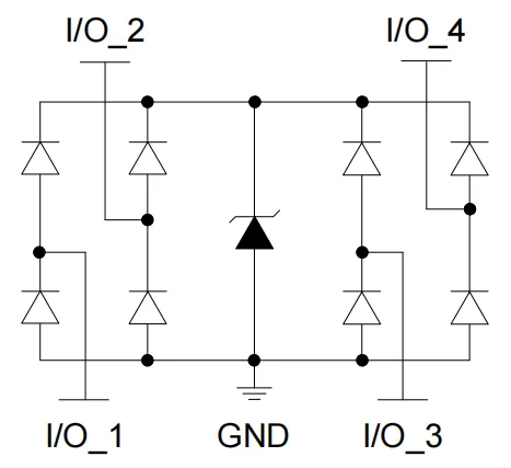
TT0314TP Internal Circuit Diagram
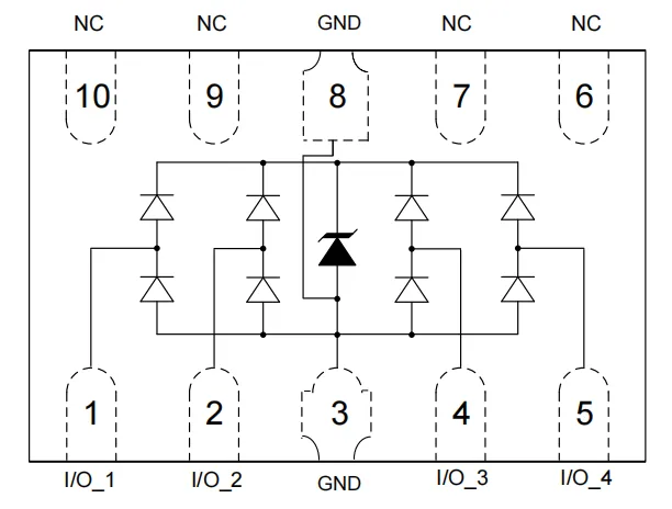
TT0314TP Pin Configuration Diagram
Through today’s discussion, we have gained a preliminary understanding of ESD protection solutions for smart bands. From protection design to component selection, every detail safeguards the stable operation of the device.