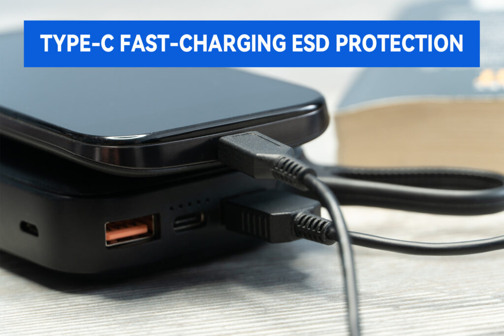
With the rapid proliferation of the USB Power Delivery (PD) protocol, the Type-C connector has become the standard interface across smartphones, notebooks, and fast-charging power adapters. Power levels have escalated from the Standard Power Range (SPR, 15–60 W) to the Extended Power Range (EPR, up to 240 W at 48 V / 5 A). While delivering accelerated charging experiences, this voltage escalation introduces increasingly severe electrostatic discharge (ESD) and electrical overstress (EOS) threats to downstream controller integrated circuits. Addressing this critical design challenge, JY Electronics has introduced a 15 V ultra-low capacitance TVS protection portfolio—the TS1501SA-W and TS1521VB-F—engineered to safeguard USB 3.x high-speed differential pairs (Tx/Rx) and USB 2.0 differential channels (DP/DM), respectively. This dual-device strategy achieves concurrent assurance of misalignment voltage withstand capability and high-speed signal integrity.
I. Protection Challenges in Type-C Interfaces: Misalignment Voltage Risk
The high-density pinout of the Type-C connector introduces inherent protection complexities. Referencing the pin assignment diagram:
Tx/Rx Channel Risk: High-speed signal pins including TX1− and RX2− are positioned adjacent to VBUS power pins. Insertion misalignment or foreign object intrusion can couple VBUS voltage directly onto signal traces.
DP/DM Channel Risk: D+/D− differential pins are similarly proximate to power pins, creating latent VBUS short-circuit vulnerability.
Voltage Escalation: Under USB PD protocol, VBUS reaches 20 V in SPR mode; in EPR mode, this extends to 28 V, 36 V, and ultimately 48 V.
Conventional 5 V-rated ESD protection devices will experience erroneous trigger conduction or catastrophic thermal failure under such misalignment scenarios. Consequently, protection components for fast-charging interfaces must exhibit 15 V working voltage capability—maintaining rapid ESD response while withstanding misalignment voltage stress. This design imperative defines the foundational architecture of the JY Electronics 15 V TVS series.
II. Differentiated Product Positioning
JY Electronics has developed precisely matched protection solutions aligned with the distinct characteristics of each channel type:

TS1501SA-W: Deep Snapback Device for USB 3.x Tx/Rx Protection
0.45 pF Ultra-Low Capacitance: USB 3.x signaling operates at 10 Gbps-class data rates. The 0.45 pF capacitance introduces negligible insertion loss on high-speed differential pairs, fully preserving signal integrity.
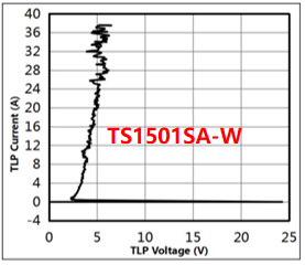
Low Clamping Voltage + High Surge Current: Peak pulse current (I_PP) reaches 20 A with a clamping voltage of merely 6.6 V. The deep snapback architecture enables rapid conduction for ESD energy dissipation while suppressing residual voltage to minimal levels, providing robust protection for sensitive controller ICs.
30 kV Protection Level: Both contact and air discharge ratings achieve 30 kV, substantially exceeding IEC 61000-4-2 requirements.
Transmission Line Pulse (TLP) characterization curves further validate the device’s ability to maintain low clamping voltage under high-current stress conditions.
TS1521VB-F: Shallow Snapback Device for USB 2.0 DP/DM
For lower-data-rate USB 2.0 DP/DM channels, the shallow snapback TS1521VB-F prioritizes misalignment
voltage withstand:
Misalignment-Tolerant Design: Trigger voltage of 22 V and clamping voltage of 19 V ensure the device remains in cutoff state during VBUS misalignment events, preventing erroneous conduction.
Signal Integrity Assurance: 1.4 pF capacitance presents no degradation to 480 Mbps USB 2.0 signaling.
22 kV ESD Rating: Satisfies standard protection requirements for consumer electronics applications.
III. Core Value of Snapback Architecture
Both devices employ snapback-structured TVS designs—a fundamental distinction from conventional
Zener-based ESD suppressors:
Deep Snapback: Post-trigger voltage collapses rapidly to a low holding level, optimal for applications demanding minimal residual voltage and high discharge capability. The TS1501SA-W exemplifies this topology.
Shallow Snapback: Relatively higher clamping voltage, optimized for channels where misalignment voltage withstand is the primary design constraint. The TS1521VB-F implements this architecture.
Through this deep/shallow snapback product stratification, JY Electronics achieves precise coverage of divergent channel protection requirements.
IV. Application Value Summary
The core competitive advantage of the JY Electronics 15 V ultra-low capacitance TVS series lies in simultaneously resolving three critical design conflicts in Type-C fast-charging applications:
Misalignment Voltage Protection vs. Erroneous Triggering: 15 V working voltage confidently addresses VBUS short-circuit risk without false conduction.
ESD Protection vs. High-Speed Signal Integrity: 0.45 pF / 1.4 pF ultra-low capacitance enables “lossless protection” with negligible impact on insertion loss and return loss budgets.
Protection Performance vs. Compact Layout: CSP0603 and DFN1006 ultra-small form factors accommodate high-density PCB designs in smartphones and fast-charging adapters.
For manufacturers of fast-charging power supplies, smartphones, and TWS charging cases, this portfolio delivers a mature, drop-in protection solution covering the full USB PD power spectrum—enhancing product reliability while reducing field failure and warranty return risk.
……………………………………………………………………Company Profile……………………………………………………………………
JY Electronics serves a global customer base across the automotive, industrial & power, computing, consumer, and mobile & wearables industries. Our extensive product portfolio includes Schottky diodes, TVS and ESD protection devices, MOSFETs, LDOs, power ICs, battery protection & segment driver ICs, industrial & automotive-grade sensors, high-side switches (HSD), current sensors, and automotive switch input chips. We are committed to continuous innovation, delivering high-quality products that empower our customers to develop energy-efficient and sustainable solutions.
For samples or a quotation, please contact us at market@jy-electronics.com.cn.